Microwave Multiphysics Laboratory
The microwave multiphysics labatory is dedicated to developing and improving the performance of semiconductor devices. These devices are all around us and support our modern lifestyle. They find applications in mobile communications, radar, power conversion, healthcare, industrial settings, defense applications, and even in next generation quantum devices.
Our aim is to substaintially improve their energy efficiency and overall performance. Essential to this mission is to understand the coupling that occurs between device physics, thermodynamics and electromagnetism. The laboratory is focused on develop new simulation algorithms/techniques and innovative measurements to quantitatively visualize the physics that surround us.
Once we see and understand it – we then seek to control it.
Multiphysics Measurements
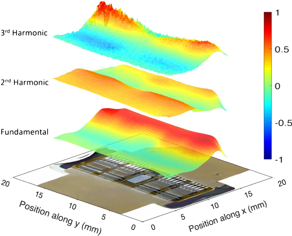
Simulation techniques are widely used but many problems are still too complex for modern simulations. We are developing new measurement techniques to see how complex circuits operate. Our measurement techniques are being employed for new 5G phones and base-stations, mm-wave antennas, and power conversion circuits. Research entails developing measurement systems, calibration, and uncertainty quantification for these new measurements – both on-wafer and fixtured devices.
Image: measured electrical fields just above 200-W LDMOS power transistor operating at 2 GHz.
Power Transistor Design
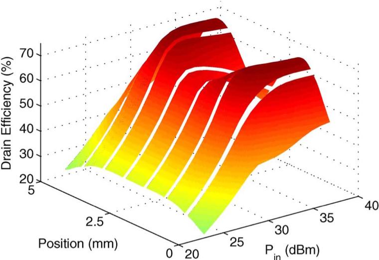
Taking advantage of the latest simulation techniques we can simulate the voltages, currents, and temperatures at all points within the power transistor. This provides incredible insight into how the transistor operates and how to optimize it. Our technques are being used for 5G GaN transistor design and very high-power silicon LDMOS for base-station amplifiers.
Image: the simulated drain efficiency across a 102-mm LDMOS transistor showing areas on the chip where the efficiency can be improved.
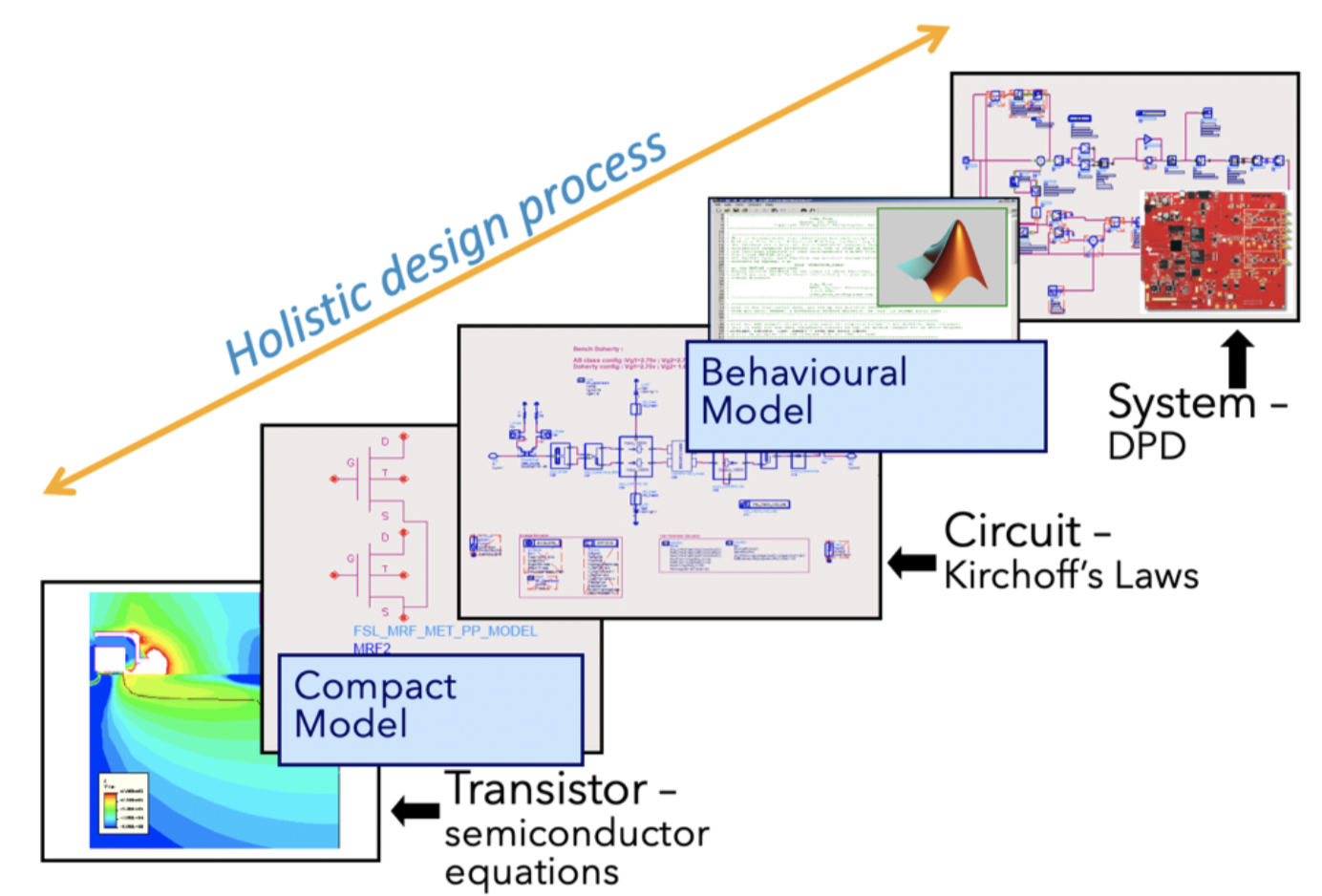
Transistor & System Modeling
We’re developing computationally efficient algorithms for LDMOS, GaN, and GaAs-based transistors that simulate thousands of times faster than conventional approaches. We combine these models with our multiphysics simulations methods. Our objective is to enable computational methods for device simulation from the device to the antenna. With efficient algorithms in place we can optimize designs and improve system-level performance.